What is a Silicon Wafer?
Silicon is a gray, brittle, tetravalent, chemical element. It makes up 27.8% of the earth’s crust and next to oxygen, it is the most abundant element in nature. Some of the most common materials that contain silicon are quartz, agate, flint, and common beach sand, among others. It is the main component in building materials like cement, brick, and glass. Silicon is also the most common material to build semiconductors and microchips with. Ironically, silicon by itself does not conduct electricity very well; however, it can take on dopants precisely in order to control resistivity to an exact specification.
Before a semiconductor can be built, silicon must turn into a wafer which becomes a silicon wafer. This begins with the growth of a silicon ingot. 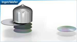 A single silicon crystal consists of atoms arranged in a three-dimensional periodic pattern that extends throughout the material. A polysilicon crystal is formed by many small single crystals with different orientations, which alone, cannot be used for semiconductor devices.
Silicon Wafer Manufacturing
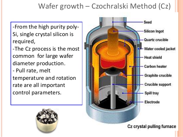
The time it takes to grow a silicon ingot varies, depending on many factors. More than 75% of all single crystal silicon wafers grow via the Czochralski (CZ) method. CZ ingot growth requires chunks of virgin polycrystalline silicon. These chunks are placed in a quartz crucible along with small quantities of specific Group III and Group V elements called dopants. The added dopants give the desired electrical properties for the grown ingot. The most common dopants are boron, phosphorus, arsenic, and antimony. Depending on the dopant, the ingot becomes a P or N type ingot (boron: P type; phosphorus, antimony, arsenic: N type).
Ingot Growth
To grow an ingot, the first step is to heat the silicon to 1420°C, above the melting point of silicon. 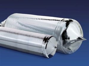 Once the polycrystalline and dopant combination has been liquified, a single silicon crystal, the seed, is positioned on top of the melt, barely touching the surface. The seed has the same crystal orientation required in the finished ingot. To achieve doping uniformity, the seed crystal and the crucible of molten silicon rotate in opposite directions. Once the system reaches proper conditions for crystal growth, the seed crystal slowly lifts out of the melt. Growth begins with a rapid pulling of the seed crystal. This minimizes the number of crystal defects within the seed at the beginning of the growing process.
After this, the pull speed reduces to allow the diameter of the crystal to increase. When the desired diameter is obtained, the growth conditions are stabilized to maintain the diameter. As the seed is slowly lifted above the melt, the surface tension between the seed and the melt causes a thin film of the silicon to adhere to the seed and then to cool. While cooling, the atoms in the melted silicon orient themselves to the crystal structure of the seed.
Slicing
Once the ingot is fully-grown, it is ground to a rough size diameter that is slightly larger than the target diameter of the final silicon wafer. The ingot has a notch or flat cut into it, in order to indicate its orientation. After passing a number of inspections, the ingot proceeds to slicing. Because of the silicon’s hardness, a diamond edge saw carefully slices the silicon wafers so they are slightly thicker than the target specification. The diamond edge saw also helps to minimize damage to the wafers, thickness variation, and bow and warp defects.
After the wafers have been sliced, the lapping process begins. Lapping the wafer removes saw marks and surface defects from the front and backside of the wafer. It also thins the wafer and helps to relieve stress accumulated in the wafer from the slicing process. After lapping the silicon wafers, they go through an etching and cleaning process. Sodium hydroxide or acetic and nitric acids alleviate any microscopic cracks and/or surface damage that may have come about during lapping. A critical edge grinding procedure takes place to round the edges, drastically reducing the probability of breakage in the remaining steps of manufacturing and later when device manufacturers use the wafers.
After rounding the edges, depending on the end user’s specification, oftentimes the edges will go through an extra polishing step, improving overall cleanliness and further reducing breakage up to 400%.
Cleaning
The final and most crucial step in the manufacturing process is polishing the wafer. This process takes place in a clean room. Clean rooms have a rating system that ranges from Class 1 to Class 10,000. The rating corresponds to the number of particles per cubic foot. These particles are not visible to the naked eye and in an uncontrolled atmosphere, such as a living room or office, the particle count would likely be 5 million per cubic foot. To help maintain this level of cleanliness, the workers must wear clean room suits that cover their body from head to toe and do not collect or carry any particles. They also stand under a fan that blows away any small particles that might have accumulated before entering the room.
Polishing
Most prime grade silicon wafers go through 2-3 stages of polishing, using progressively finer slurries or polishing compounds. The majority of the time, wafers are polished on the front side only, excluding 300mm wafers which are double side polished. Polishing produces a mirror finish. The polish also distinguishes which side to use for device fabrication. This surface must be free of topography, micro-cracks, scratches, and residual work damage.
The polishing process occurs in two steps, which are stock removal and final chemical mechanical polish (CMP). Both processes use polishing pads and polishing slurry. The stock removal process removes a very thin layer of silicon and is necessary to produce a wafer surface that is damage-free. On the other hand, the final polish does not remove any material. During the stock removal process, a haze forms on the surface of the wafer, so an extra polishing step gives the wafer a mirror finish.
After polishing, the silicon wafers proceed to a final cleaning stage that uses a long series of clean baths. This process removes surface particles, trace metals, and residues. Oftentimes, a backside scrub is done to remove even the smallest particles.
Packaging
Once the silicon wafers complete the final cleaning step, engineers sort them by specification and inspect them under high intensity lights or laser-scanning systems. This detects unwanted particles or other defects that may have occurred during fabrication. All silicon wafers that meet the proper specifications are packaged in cassettes and sealed with tape. The silicon wafers ship in a vacuum-sealed plastic bag with an airtight foil outer bag. This ensures that no particles or moisture enters the cassette upon leaving the clean room.

Anywhere in the Bay Area within 4 hours.

In the United States within 1 day.

Internationally within 3 days.