Silicon Valley Microelectronics offers a comprehensive list of photoresist products including broadband, I-Line, 248nm, 193nm, e-beam, positive, negative, wet and dry resists. SVM offers photoresist solutions for patterning & etching on all wafer diameters. Project design rules dictate a specific photoresist type/ performance. SVM handles projects associated with CMOS, MEMS, TSV, FEOL, BEOL and more. This has allowed us to create a large portfolio of photoresist types for these and other applications. SVM has a long history of patterning wafers for test-vehicle applications, engineering short-loop flow work, applying hard-baked blanket PR for use as a sacrificial protective layer, etch studies, etc. SVM supplies blanket resists via spin or spray-on for a range of applications. For questions about a specific project, please contact us at (408) 844-7100 or email us at [email protected].
SVM Photoresists available:
I-Line
I-Line is a general purpose resist film that is sensitive at 365nm in the UV light spectrum. I-Line photo resist products are often broadband resists with light sensitivity to G (435nm) and H (405nm) lines, but can also be exposed monochromatically within their spectral sensitivity. This film has excellent adhesion and plating characteristics for precise control of exposure which makes it great for use in MEMS and wafer level packaging processes such as bumping.
193nm, 248nm Deep-Ultraviolet (DUV)
For more advanced lithography applications, SVM offers DUV 248nm KrF and 193nm ArF photoresist products. Products can be applied with or without an anti-reflective coating.
Thick Photoresist and Photo Imageable Polyimide
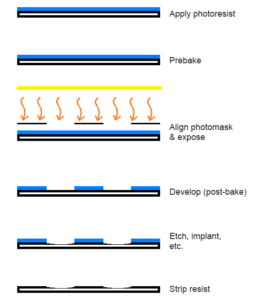
Photoresist Patterning Process:
- Substrate preparation – The substrate is cleaned, then goes through a dehydration bake and/or an adhesion promoter is added in order to prepare the wafer for the rest of the process.
- Photoresist spin coating – A thin, uniform coating made from a mixture of photoresists and solvents is deposited via spin-coating. The film is deposited either while the wafer is spinning (dynamic dispense) or not spinning (static dispense).

- Prebake – After spin-coating, 20-40% of the film is still solvent. The addition of a prebake dries the photoresist and stabilizes the film. This step reduces thickness, changes the properties of film, improves adhesion, and makes it less susceptible to particle contamination.
- Exposure – This changes the solubility of the film in order to pattern the wafer by exposing it to light. There are 3 forms of exposure:
- Contact – Mask is in contact with photoresist.
- Proximity – Mask is ~15 – 20μm above photoresist.
- Projection – Mirrors project a slit of light from the mask to the wafer surface. To determine the correct exposure, engineers measure the light intensity, slit size, and spin speed of the substrate. There are two versions of projection exposure:
- Scanning – A computer scans the wafer surface, and a light moves around to expose correct area.
- Step-and-repeat – Small areas of the wafer are exposed to light.
- Post-exposure bake – This step is generally for wafers with high resolution (<1 micron). In most other circumstances, the substrate goes straight from exposure to development.
- Development – The wafer goes through a chemical rinse to expose the etching left by the mask.
- Strip photoresist – Chemical removal or etching gets rid of all remaining photoresist to produce the final pattern on the wafer.
Not finding what you’re looking for?
If you have a question or would like to request a quote, please contact a member of our Sales Team.
Contact UsInventory
Anywhere in the Bay Area within 4 hours.

In the United States within 1 day.

Internationally within 3 days.